Trends in Semiconductor Fabrication & Innovation to Look Out for in 2021
2020 had an unprecedented impact on every industry and nation as the COVID-19 crisis caused an increase in remote work. The shift to work-from-home, however, also brought a rapid acceleration in digitalization, as businesses transformed their delivery of services worldwide to remote customers.
This transition resulted in an unforeseen uptick in the need for silicon wafers, which play a critical role in emerging technologies. Whereas in 2019, the silicon wafer market fell 6.9% due to a downturn in the memory business, global silicon wafer shipments increased by an estimated 2.4% in 2020. Looking to the future, the semiconductor market is anticipated to grow by $90.8 billion from 2020 through 2024, which represents a CAGR of over 4%. Driving this growth will be the continued rapid innovation of technologies that further digitalize our world, and that require high-performance semiconductors to run effectively.
The Emergence of Innovative Technology Solutions
Artificial Intelligence (AI) as a concept has dominated industry conversations for years, but companies—ranging from research to healthcare, high-tech, and consumer electronics—are now truly beginning to implement AI-enabled solutions in earnest. These innovative AI applications require a massive amount of data to be processed and stored in order to learn and interact with their environment. To support AI-integrated circuits, there will need to be improvements to semiconductor architectures to speed the movement of data in and out of memory with increased power and more efficient memory systems.
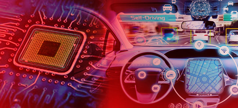
Starting in 2020, an increased focus was also placed on the emergence of 5G: next-generation wireless technology that boasts higher data transfer rates, lower latency, and the ability to support more devices. In particular, 5G will prove vital in moving the massive quantities of data generated by advanced electronics and sensors, like those used in autonomous cars and IoT devices.
In turn, components like processors, modems, and logic chips in the IoT infrastructure will need greater memory output and higher performance to sustain these next-gen applications. For the semiconductor industry—which creates the wafers that power 5G devices—this introduces greater complexity into semiconductor fabrication as a need for greater data storage, analysis, and processing power demands integrated chips (IC).
Semiconductor Wafers are Becoming Thinner & More Structurally Complex
Since the introduction of finFETS and 3D NAND, the structure of semiconductors has become increasingly intricate—a trend poised to continue as 5G develops. In particular, a greater number of chips are being stacked on one another to increase memory or achieve complex heterogenous integration, resulting in both more complicated structures and more possibilities for points of failure. When operating at the nanometer level, it can be particularly challenging to pinpoint what causes a failure.
To ensure technology performs optimally throughout its expected lifetime, especially when used in mission-critical applications like self-driving vehicles, medical devices, or industrial robots, chipmakers must ensure that no contaminates are introduced during production that could compromise quality or worse, create latent defects. These imperceptible flaws can be caused by the slightest impurity, but can have significant safety consequences if the semiconductor fails in use. And, this exacting level of gas purity must be upheld while handling higher volumes of gas than ever, as fabs must continue to ramp production to keep up with market demand.
This requires the use of high-performance gas delivery equipment than can uphold the integrity of process gases at scale. For instance, in a 3D NAND fab, 80,000 – 100,000 Nm3/h of 99.999% pure nitrogen is required. Semiconductor fabs will need to ensure not only that their ultra high purity process gases can be handled at every phase of production without introducing impurities, but that equipment can maintain this level of purity even at high gas volumes. Gas purifiers are imperative to attaining gas purification to the parts per billion (PPB) or even parts per trillion (PPT) level, with industry-leading solutions able to attain up to 10Ns (99.99999999%) of purity.
Where is Industry Innovation Heading?
Looking ahead to market trends for 2021, the 300mm silicon wafer market is expected to increase in 2021 by 5% in comparison to 2020. In particular, 300mm epitaxial wafers, which are used for logic devices, are predicted to be in the greatest demand when compared to memory and polished wafers. To support this demand, fabs will again require proven gas delivery equipment that can meet stringent needs for purity and precision.
As we enter into the New Year with a positive outlook for the semiconductor market, AES is poised to provide the gas delivery systems and partnership that semiconductor and electronics manufacturers need to produce the components powering the future of innovation.
Energize your own innovation with a Starbucks drink, on us! Fill in the form for a $5 Starbucks gift card, then contact us to discuss your business needs.
Share this Post: